


Electronic devices constantly get smaller – and more powerful. To fit more transistors on a silicon chip, engineers have to design smaller transistors. The first chip had about 2,200 transistors on it. Today, hundreds of millions of transistors can fit on a single microprocessor chip.
Even so, chip-manufacturing companies are determined to create increasingly tiny transistors, cramming more into smaller chips. There are already computer chips that have nanoscale transistors (nanoscale is between one and 100 nanometers; a nanometer is one billionth of a meter), and in the future, transistors will have to be even smaller.
To fill the gap, the nanowire – a structure that has an amazing length-to-width ratio and incredibly thin – was invented. It’s possible to create a nanowire with the diameter of just one nanometer, though engineers and scientists tend to work with nanowires that are between 30 and 60 nanometers wide. Scientists hope that we will soon be able to use nanowires to create the smallest transistors yet, though there are some pretty tough obstacles in the way.
Perhaps the most common use for nanowires is in electronics; there are hundreds of potential nanowire applications in electronics. Researchers in Japan are working on atomic switches that might someday replace semiconductor switches in electronic devices. Some nanowires are very good conductors or semiconductors, and their minuscule size means that manufacturers could fit millions more transistors on a single microprocessor. As a result, computer speed would increase dramatically
Now, researchers at the Technion-Israel Institute of Technology in Haifa have presented an innovative method for the formation of nanowires. In it, the nanowires form within line defects that exist in metals. Such defects are known as dislocations. This is the first time that dislocation lines in a material of one kind serve as a template for the growth of a different inorganic material in the form of nanowires. The study, which was published in PNAS (Proceedings of the [US] National Academy of Sciences) under the title “Self-catalytic growth of one-dimensional materials within dislocations in gold.”
The research was led by Prof. Boaz Pokroy and doctoral student Lotan Portal of the Faculty of Materials Science and Engineering and the Russell Berrie Nanotechnology Institute (RBNI).
Dislocations are a significant phenomenon in materials science since they affect the material’s properties on both the macro- and microscales. For example, a high dislocation density increases a metal’s strength and hardness. The dislocation edges on metal surfaces and the atoms in their proximity tend to be more chemically activated compared to other atoms in the material and tend to facilitate various chemical reactions, such as corrosion and catalysis.
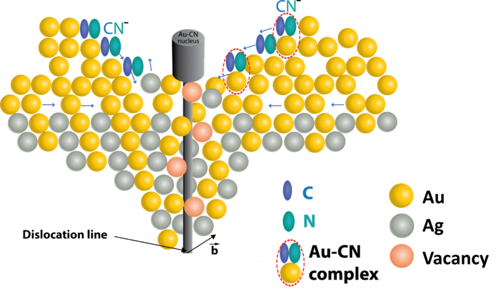
The Technion team created nanowires of gold-cyanide complex from classic Au-Ag alloy. In professional terminology, they synthesized inorganic gold(I)-cyanide (AuCN) systems in the shape of nanowires, using an autocatalytic reaction through the acceleration of a reaction by one of its reactants. Gold-cyanide complex is used in numerous fields including ammonia-gas detection, catalysis (acceleration) of water-splitting reactions and others.
In the process developed by the researchers, nanowires crystallize at the dislocation ends on the surface of the original gold-silver (Au-Ag) alloy, and the final structure obtained is classic nanoporous (sponge-like) gold, with a layer of nanowires emerging from it. Formation of the nanowires occurs during the classic selective dealloying process that separates the silver from the system and forms the nanoporous gold and is achieved only when the dislocation density exceeds a critical value, as presented in the kinetic model developed and demonstrated in the article.
The model provides a possible route for growing one-dimensional inorganic complexes while controlling the growth direction, shape, and morphology of a crystal according to the original alloy’s slip system. As mentioned, this scientific and technological achievement has numerous potential applications.
The shortcode is missing a valid Donation Form ID attribute.